V-Scoring
Introduction
The V-Scoring process allows for the penalizing of PC boards, which facilitates convenient handling, assembly and soldering. V-Scoring is essential for SMD (surface mount devices) PC boards, where pick and place assembly methods are used. The PCB panel to be V-Scored consists of several PC boards which have been manufactured in an array, i.e. stepped and repeated several times on either or both the X axis and the Y axis.
Tolerance of the Nominal Breaking Point
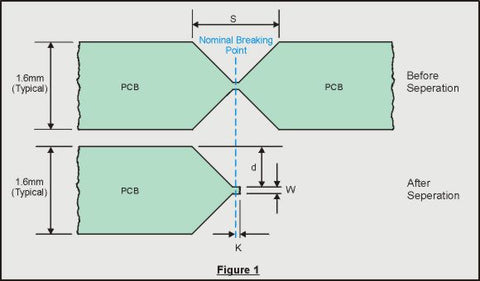
When the scored panel is broken up into individual PC boards, an "increase" in the size of the profile occurs. This "increase" is determined by the nominal breaking point, and the geometry of the cutting blade used to separate the PC boards. For PC boards of 1.6mm thick, the typical web thickness (w in fig. 1) is 0.3mm, and the "increase" is between 0.1mm and 0.15mm (k in fig. 1). Note that this "increase" occurs on all sides of the PC board, so the total increase in board size is 2 X k. Therefore, after seperating the PC boards the dimensions will have increased by between 0.2 mm and 0.3 mm.
Width of the Score at the PC Board Surface
The width of the score (s in fig.1) depends upon the thickness of the material used but generally varies between 0.3mm and 0.6mm for 1.6mm thick PC boards, depending on the variations of the material thickness. As a result, a gap has to be left between the PC boards for V-Scoring which results in a slight increase in the cost of the PCB.